ADN4662 Single, 3 V, CMOS, LVDS Differential Line Receiver
09/23/2022
Product Details
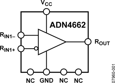
The ADN4662 is a single, CMOS, low voltage differential signaling (LVDS) line receiver offering data rates of over 400 Mbps (200 MHz), and ultralow power consumption. It features a flow-through pinout for easy PCB layout and separation of input and output signals.
The device accepts low voltage (310 mV typical) differential input signals and converts them to a single-ended 3 V TTL/ CMOS logic level. The ADN4662 and its companion driver, the ADN4661, offer a new solution to high speed, point-to-point data transmission, and a low power alternative to emitter-coupled logic (ECL) or positive emitter-coupled logic (PECL).
Applications
- Point-to-point data transmission
- Multidrop buses
- Clock distribution networks
- Backplane receivers
Features and Benefits
- ±15 kV ESD protection on input pins
- 400 Mbps (200 MHz) switching rates
- Flow-through pinout simplifies PCB layout
- 2.5 ns maximum propagation delay
- 3.3 V power supply
- High impedance outputs on power-down
- Interoperable with existing 5 V LVDS drivers
- Accepts small swing (310 mV typical) differential signal levels
- Supports open, short, and terminated input fail-safe
- 0 V to −100 mV threshold region
- Conforms to TIA/EIA-644 LVDS standard
- Industrial operating temperature range: −40°C to +85°C